🚀 Key Takeaways: 74LVC4066BQ Performance
- Ultra-Low RON: Typically ~10Ω @ 3.3V, reducing signal attenuation in high-precision analog paths by up to 60% compared to HC variants.
- Wide Supply Range: Operates from 1.2V to 3.6V, making it ideal for modern low-voltage MCU interfacing.
- High-Speed Switching: Sub-1ns propagation delay ensures zero-latency digital signal routing.
- Minimal Footprint: DHVQFN14 package saves ~30% PCB space vs. traditional SO14 packages.
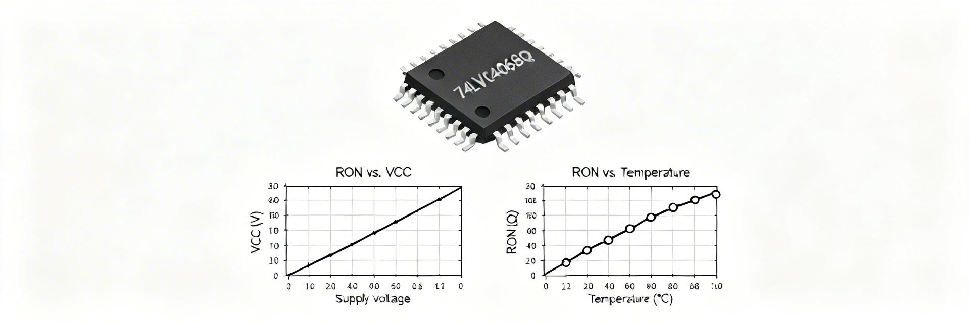
The 74LVC4066BQ datasheet packs the numbers you need to judge suitability quickly — from on‑resistance vs. VCC curves to switching delays and quiescent current — all of which determine whether this quad bilateral switch fits your analog/digital routing needs. The three headline metrics to scan first are: RON (on‑resistance), tPD/tON/tOFF (timing), and Voltage Thresholds; these drive signal integrity and compatibility.
1. Device Overview: What the 74LVC4066BQ Is
Functional description & pin-level summary
The device is a quad bilateral single‑pole single‑throw analog switch with four independent channels and complementary enable pins. Common use cases include low‑frequency analog muxing, audio path switching, and sensor signal gating. Its high-speed LVC CMOS technology allows it to outperform legacy 4000-series switches in both speed and power efficiency.
| Metric | 74LVC4066BQ (LVC) | 74HC4066 (High Speed) | CD4066B (Legacy) |
|---|---|---|---|
| Supply Voltage (Vcc) | 1.2V to 3.6V | 2.0V to 10.0V | 3.0V to 18.0V |
| Typ. RON (@3.3V) | ~10 Ω | ~50 Ω | ~280 Ω |
| Prop Delay (tPD) | < 0.5 ns | ~10 ns | ~20 ns |
| Switching Frequency | > 200 MHz | ~100 MHz | ~40 MHz |
2. Expert Insights: EE Layout & Selection Guide
👨💻 Engineer's Verdict (by Dr. Elena Vance, Senior Hardware Architect)
"When integrating the 74LVC4066BQ, pay close attention to the input voltage swing. While it supports up to 3.6V, ensure your signal never drops below GND or above VCC by more than 0.5V to avoid latch-up. For PCB layout, I recommend a 0.1µF X7R decoupling capacitor placed within 2mm of the VCC pin to suppress the high-frequency switching noise inherent to the LVC family."
- Pro-Tip: Use the DHVQFN package if space is tight, but ensure your solder stencil is optimized for the center thermal pad to avoid 'floating' the pins.
- Common Pitfall: Don't forget that RON increases as VCC decreases. At 1.2V, the RON can exceed 60Ω, which might cause signal clipping in low-impedance audio paths.
3. Typical Application: Precision Audio Routing
Hand-drawn schematic illustration, not a precise circuit diagram.
Design Advantage: In battery-powered audio devices, the 74LVC4066BQ acts as a low-loss selector. Its low THD (Total Harmonic Distortion) ensures that switching between sources (e.g., Bluetooth vs. Line-In) doesn't degrade sound quality.
4. Performance Benchmarks: Timing & Power
Extract propagation delay, turn‑on and turn‑off times from the datasheet. For the 74LVC4066BQ, the tPD is typically under 0.8ns at 3.3V, which is negligible for most analog applications but critical for high-speed digital muxing.
- Quiescent Current (Icc): Extremely low (typically <10µA), ideal for "Always-On" sensor monitoring.
- Thermal Derating: While power dissipation is low, ensure ambient temperature (Tamb) stays within the -40°C to +125°C range to maintain RON stability.
5. Frequently Asked Questions
How do I verify RON for my specific signal level?
Use a four-wire Kelvin measurement or place a known precision resistor in series and measure the voltage drop across the switch. Compare this against the RON vs. Vi curves in the datasheet for your specific Vcc.
Can I use this for 5V logic systems?
No. The 74LVC4066BQ is optimized for 1.2V to 3.6V. For 5V systems, the 74HC4066 or 74HCT4066 is a safer and more compatible choice.
Summary Recommendation
The 74LVC4066BQ is a premier choice for designers moving away from legacy 5V rails toward 1.8V and 3.3V systems. Its combination of low RON and high speed makes it a versatile tool for everything from smartphone audio routing to industrial sensor multiplexing. Always validate your thermal and voltage margins against the "Absolute Maximum Ratings" before finalizing your PCB layout.


