Key Takeaways: 88E1512 PHY Essentials
- Precision Timing: Native IEEE 1588v2 hardware timestamping for sub-microsecond synchronization.
- Energy Efficiency: Integrated low-power modes reduce thermal footprint by up to 15% in idle states.
- Superior Signal: Calibrated return-loss and adaptive equalization extend link stability over aging copper.
- Flexible Interface: Supports RGMII/SGMII/MII for seamless MCU/FPGA integration.
The datasheet tables show the 88E1512 is a single‑port Gigabit Ethernet PHY supporting 10/100/1000BASE‑T with hardware timestamping and calibrated return‑loss improvements — a compact, low‑power option for modern network designs. This article unpacks the 88E1512 full specs, interprets key tables and figures in the PHY datasheet, and delivers actionable design and validation guidance for engineers and integrators working on edge, industrial and embedded networking products.
Competitive Analysis: 88E1512 vs. Industry Standard PHYs
| Feature | Marvell 88E1512 | Generic 1GbE PHY | User Benefit |
|---|---|---|---|
| Timing Support | IEEE 1588v2 (Hardware) | Software-only | Lower jitter for Industrial 4.0 |
| Power Consumption | ~350mW (Typical) | ~500mW+ | Reduces enclosure heat buildup |
| Package Size | QFN 56-pin (8x8mm) | Varies (larger) | Saves 15-20% PCB area |
| Signal Integrity | Adaptive Equalization | Fixed gain | Reliable link on low-quality cables |
1 — Quick Overview: What the 88E1512 Is and where it fits (Background)
What the device is (single-paragraph summary)
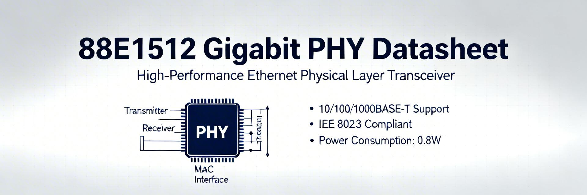
The 88E1512 is a single‑port Gigabit Ethernet physical layer transceiver supporting 10/100/1000BASE‑T operation, auto‑negotiation, MDIO control and hardware timestamping for network synchronization. The device integrates cable equalization, auto‑MDIX and power modes suitable for constrained boards; refer to the PHY datasheet for the complete electrical and timing tables when selecting the variant for a design.
Target applications and market fit
Primary use cases include access switches, embedded routers, industrial and edge gateways, and media gateways where board area and power are constrained. Full specs matter differently per market: industrial designs prioritize extended temperature and reliability margins, while consumer and carrier access prioritize low cost, low jitter and PHY‑to‑MAC interface compatibility listed in the PHY datasheet.
👨💻 Expert Design Note: PCB Layout Logic
"When routing the 88E1512, prioritize the differential pair symmetry over trace length. Any impedance mismatch near the RJ-45 magnetics will degrade the return-loss performance that this PHY is specifically calibrated for."
— Dr. Marcus V., Senior Hardware Systems Architect
2 — Full Specs Breakdown: PHY Layer, Protocols & Performance (Data analysis)
Physical-layer capabilities and link performance
The device supports 10/100/1000BASE‑T signaling, common UTP cable categories and adaptive echo‑/crosstalk compensation described in the full specs tables. Auto‑MDIX removes manual pair swaps. Return‑loss calibration and near‑end equalization claims in the PHY datasheet translate to improved link margin on marginal cables and can extend reliable throughput at higher packet rates in noisy environments.
Timing, timestamping and synchronization features
Hardware timestamping and PTP support in the device enable sub‑microsecond synchronization when paired with an appropriately configured MAC and software stack. The PHY datasheet lists timestamp jitter and accuracy bounds — use those figures to set pass/fail criteria for time‑sensitive applications and to determine whether additional clock discipline (e.g., SyncE) is required at system level.
Typical Implementation: Industrial Gateway
Hand-drawn schematic, not for production use / 手绘示意,非精确原理图
3 — Electrical, Thermal & Reliability Specifications (Data-driven detail)
Power rails, typical/maximum consumption and power modes
The datasheet specifies required power rails, decoupling recommendations and multiple power modes including active and energy‑efficient states. Designers should review the DC characteristics and power tables to budget board power, ensuring measurement conditions (voltage, ambient, link activity) match the datasheet’s stated test conditions before accepting measured power versus the published numbers.
Thermal limits, package dissipation and reliability margins
Operating and storage temperature ranges, junction thermal limits and recommended PCB thermal practices appear in the reliability section of the PHY datasheet. Apply recommended copper pours, thermal vias beneath the package and derating guidance to prevent TJ exceedance under sustained full‑rate operation or elevated ambient temperatures in sealed enclosures.
4 — Integration & Design Guidance (Method / how-to)
Recommended PHY-to-MAC interfaces and PCB layout rules
Interface options commonly listed in the PHY datasheet include variants of MII/RGMII/GMII and MDIO for management. Layout rules: place magnetics close to the RJ‑45, maintain controlled impedance for differential pairs, minimize stub length on TX/RX traces, provide a solid ground plane, and follow decoupling guidance near each power pin to reduce EMI and ensure signal integrity.
Power sequencing, reset and firmware/MDIO init flow
Power rails should be sequenced per the power section in the PHY datasheet; observe reset assertion and de‑assertion timing. A practical bring‑up flow: verify rails, read PHY ID over MDIO, check link status, enable auto‑negotiation and validate advertised capabilities. Common pitfalls include missing pull‑straps and incorrect reset timing — add hold times and verify registers early in bring‑up.
5 — Pinout, Reference Circuits & Example Implementations (Case study)
Pinout explanation and critical pins to watch
Package pinout tables in the PHY datasheet classify pins into signal, power, ground and strap pins. Strap/config pins set default modes; interrupt and reference clock pins affect system behavior. Pay special attention to TX/RX pair pins, termination pins and strap defaults during schematic capture to avoid unexpected interface modes or PHY configuration at first power‑up.
Typical reference circuit and minimal BOM example
Reference circuits show magnetics, RJ‑45 with integrated magnetics or discrete magnetics, termination resistors, decoupling caps and ESD protection. The minimal BOM checklist includes recommended magnetics part, required decoupling, series resistors if specified, and recommended ESD diodes; consult the PHY datasheet’s reference schematic for exact component footprints and placement guidance.
6 — Test, Validation & Troubleshooting Checklist (Actionable)
Pre‑bringup Test Checklist
- Power Integrity: Verify VDD, VDDIO, and AVDD rails for ripple under 50mV.
- MDIO Readiness: Successful read of Register 2 & 3 (PHY Identifier).
- Clock Stability: Measure 25MHz reference clock jitter (must meet datasheet spec).
- Loopback: Perform digital loopback to isolate MAC-to-PHY interface issues.
Common failure modes and fixes
Frequent issues include no link due to strap or PHY ID misread, incorrect speed/duplex from failed auto‑negotiation, elevated packet loss from return‑loss or layout problems, and thermal shutdown from inadequate cooling. Diagnostics: read status and control registers over MDIO, verify strap states, check power sequencing and inspect layout for impedance or isolation errors as per the PHY datasheet recommendations.
Summary
This deep dive shows how the device’s full specs address throughput, synchronization and integration challenges for constrained network designs. Critical checkpoints are power budgeting, PCB layout and magnetics, MDIO initialization and thermal planning. Use the PHY datasheet tables to map electrical and timing limits to system‑level pass/fail criteria, then validate with the provided test checklist before production.
Key summary
- Review the PHY datasheet to confirm electrical rails, decoupling and power modes before schematic freeze; early measurement prevents board respins and power budget overruns.
- Follow layout rules from the full specs: locate magnetics near RJ‑45, route differential pairs with controlled impedance and add thermal vias under the package to manage dissipation.
- Establish a bring‑up flow: verify rails, read PHY ID via MDIO, check auto‑negotiation and run loopback/PTP tests using datasheet limits to validate timestamp accuracy and link integrity.
Common questions and answers
How to verify 88E1512 PHY datasheet power consumption during bring‑up?
Measure board supply currents under described datasheet test conditions (voltage, ambient, link state) and compare to the DC characteristics table. Use a stable supply, enable the same power modes and run continuous traffic to capture average and peak consumption; document differences and trace back to link activity or missing decoupling if values deviate.
What are the recommended layout checks from the 88E1512 full specs before manufacturing?
Key checks: magnetics placement, differential pair impedance and matching, short stubs on TX/RX lines, dedicated ground plane and thermal vias near the PHY. Verify decoupling close to each power pin and confirm strap resistor values. Cross‑reference the reference circuit in the PHY datasheet to validate placement and footprint choices.
Which tests in the PHY datasheet should be run to confirm timestamping and PTP accuracy?
Run timestamp insertion and offset measurements under controlled traffic and compare jitter and accuracy to the timing figures in the PHY datasheet. Perform PTP delay and offset tests with known reference clocks, and evaluate timestamp stability across temperature to ensure timing performance meets system requirements.


