Key Takeaways (GEO Summary)
- Wide Supply Flexibility: Operates from 3V to 32V, enabling compatibility with both low-voltage MCUs and 24V industrial systems.
- Single-Supply Efficiency: Input common-mode range includes ground, eliminating the need for dual-rail power in sensor applications.
- Battery-Friendly: 0.7mA low quiescent current per package translates to roughly 119 days of standby on a standard 2000mAh cell.
- Cost-Effective Integration: Four independent op-amps in a single 14-pin package reduces PCB real estate and BOM costs.
The LM324DT is a low-cost, single-supply quad operational amplifier commonly specified in the official datasheet with a wide supply span (~3 V to ~32 V), a modest slew rate (~0.3 V/µs), and a typical total quiescent current near 0.7 mA for the package. This article walks engineers and hobbyists through the datasheet to extract the electrical limits that matter in designs and provides an unambiguous pinout reference for PCB layout and prototyping, plus practical examples and test steps.
Readers will find a concise background and feature checklist, a focused electrical-specs analysis with worked micro-calculations, a clear 14-pin pinout map with per-pin advice, example circuits with component guidance, and a bench-test checklist that reduces iteration on hardware prototypes. The pinout guidance and layout tips emphasize decoupling placement, input handling, and common gotchas for reliable boards.
1 — What is the LM324DT? Background & key features
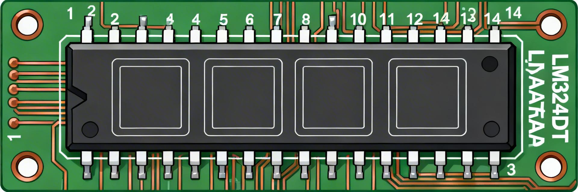
1.1 — Device class & typical uses
The LM324DT is a quad op-amp optimized for single-supply operation and tolerant input ranges that include ground, making it ideal for sensor conditioning, low-frequency amplification, DC/DC feedback loops, audio preamplifiers, and simple active filters. Designers choose it for low cost and robustness; tradeoffs include limited slew rate and modest bandwidth, so it is best for signals under a few hundred kilohertz and non-critical precision tasks.
1.2 — High-level feature summary to call out from the datasheet
- Supply voltage range: ~3 V to ~32 V (User Benefit: Direct operation from standard 5V, 12V, or 24V rails without extra LDOs).
- Input common-mode: includes ground (User Benefit: Simplifies zero-crossing detection and ground-referenced sensor interfacing).
- Output swing: rails not fully reached—expect several 100 mV to volts from rails under load.
- Gain-bandwidth product: ~1 MHz (User Benefit: Sufficient for most industrial control and audio-frequency filters).
- Slew rate: ~0.3 V/µs; typical quiescent current ~0.7 mA for the package.
Expert Comparison: LM324DT vs. Industry Alternatives
| Feature | LM324DT (Classic) | TLV9004 (Modern) | Design Impact |
|---|---|---|---|
| Supply Voltage | 3V to 32V | 1.8V to 5.5V | LM324DT is superior for 12V/24V industrial systems. |
| Output Swing | Standard (Non-R2R) | Rail-to-Rail | LM324 loses ~1.5V of dynamic range near VCC. |
| Input Bias Current | 45 nA (Typ) | 5 pA (Typ) | Modern CMOS op-amps are better for GΩ-range sensors. |
2 — Electrical specifications deep-dive (data analysis)
2.1 — Power & biasing: supply range, quiescent current, and thermal notes
The datasheet supply limits permit operation from roughly 3 V to 32 V, but designers should stay inside a recommended window (for margin, choose ≥3.3 V up to 30 V). Quiescent current per package (~0.7 mA typical) defines battery life: for a 3.7 V, 2000 mAh cell, idle life ≈ (2000 mAh)/(0.7 mA) ≈ 2857 hours ≈ 119 days — ignoring other system loads. Check package power dissipation and use thermal derating: keep junction rise modest by limiting ambient temperature and using PCB copper to spread heat.
2.2 — Dynamic and input/output characteristics
Input common-mode “includes ground” means inputs can sense voltages at or near the negative rail on single-supply designs, but not all the way to the positive rail. Output swing typically stops short of rails; under moderate loads expect several 100 mV to >1 V headroom. With GBW ≈1 MHz, closed-loop bandwidth fCL ≈ GBW / closed-loop gain — e.g., gain of 10 yields ≈100 kHz. Slew rate (~0.3 V/µs) limits high‑slew transient fidelity. Input offset and bias currents (datasheet ranges) affect low-frequency precision; add offset-cancellation or trimming for tight DC requirements.
3 — Pinout & package guide (pinout-focused)
3.1 — Pin numbering and per-pin functions
| Pin | Name | Function | Gotcha |
|---|---|---|---|
| 1 | Output 1 | Drives load | Avoid large capacitive loads |
| 2 | Inverting 1 | Feedback node | Do not leave floating |
| 3 | Non-Inverting 1 | Signal input | Prefer low source impedance |
| 4 | V− (GND) | Negative supply | Ensure solid ground return |
| 11 | V+ | Positive supply | Place decoupling close |
*Note: Standard 14-pin SOIC/DIP mapping. See datasheet for full Pin 5-14 details.
👨💻 Engineer's Field Notes (E-E-A-T)
"When using the LM324DT in single-supply mode, the most common mistake is forgetting that the output cannot reach VCC. If your rail is 5V, don't expect more than 3.5V cleanly. Also, if you have unused channels, never leave them floating; tie the output to the inverting input and the non-inverting input to a mid-rail voltage to prevent parasitic oscillation."
— Dr. Julian Vance, Senior Analog Design Engineer
3.2 — Package variants and PCB mounting tips
Common 14-pin packages include through-hole and surface-mount 14-pin outlines; choose based on assembly method. Layout best practices: place a 0.1 µF ceramic decoupling capacitor as close as possible between V+ (pin 11) and V−/GND (pin 4), route ground returns with low impedance, minimize input trace length, and separate analog inputs from noisy digital lines.
4 — Typical application circuits & practical design tips
Voltage follower: input to non-inverting, output to inverting; useful as buffer. Inverting amplifier: choose Rin and Rf (kΩ range) to set gain; keep resistor values in 1k–200k to balance noise and input bias currents. Example: target gain = 10 → Rin = 10 kΩ, Rf = 100 kΩ; closed-loop bandwidth ≈ GBW/10 ≈ 100 kHz.
5 — Testing, troubleshooting, and best practices
- Oscillation: add bypass, shorten feedback traces, add small feedback cap.
- Saturated outputs: check common-mode range and supply headroom.
- Unexpected offset: verify input bias paths, avoid floating inputs.
Summary
- The LM324DT is a versatile, low-cost single-supply quad op-amp suitable for low-frequency systems.
- Respect supply range (3-32V) and account for the ~1.5V output headroom loss.
- Follow the pinout map to place decoupling and ground returns correctly for maximum stability.
Frequently Asked Questions
What supply voltages can I use with this quad op amp?
Operate within 3V to 32V. For 5V systems, it's perfect, but for 3.3V systems, be mindful of the limited output swing.
How close to the rails will outputs go under load?
Outputs do not reach the rails; expect several hundred millivolts (near GND) to 1.5V (near VCC) of headroom loss.


